- 您现在的位置:买卖IC网 > Sheet目录1219 > HC5514XEVAL3 (Intersil)EVAL BOARD TI CODEC MOTHER BOARD
�� �
�
�Application� Note� 9871�
�3.� Con?gure� the� SLIC� to� be� in� the� Ringing� State�
�(C3� =� 0,� C2� =� 0,� C1� =� 1).�
�4.� Con?gure� S5� and� S6� to� be� in� the� LED� position.�
�5.� Verify� that� the� POL/REV� pin� S4� (lower� right� hand� side� of�
�the� board)� is� in� either� the� 10ms� or� 20ms� position.�
�6.� Connect� the� telephone� across� tip� and� ring.�
�7.� Ground� the� RSYNC_REV� terminal.�
�8.� Connect� battery� backed� AC� (20Hz,� 90V� RMS� +V� BH� )�
�source� to� “RINGING”� located� just� below� the� tip� and� ring�
�terminals� on� the� board.�
�Veri?cation�
�1.� Phone� starts� ringing� when� power� is� applied� to� the� test�
�setup;� if� not,� toggle� C1.�
�2.� While� ringing� and� Onhook,� SHD� LED� is� not� illuminated.�
�3.� While� ringing,� going� offhook� will� illuminate� the� SHD� LED.�
�When� an� offhook� condition� is� detected,� the� HC5514X� will�
�automatically� disable� the� RRLY� pin� (pin� goes� high)� at� zero�
�current� crossing.� This� will� disable� the� ring� relay� and�
�reconnect� the� tip� and� ring� lines� to� the� phone.�
�4.� When� the� phone� is� returned� to� the� Onhook� condition,�
�SHD� light� will� remain� on� until� the� logic� state� of� the� SLIC�
�is� changed.� This� precludes� any� false� on� hook� detection�
�during� the� transition� between� off� hook� (during� ringing)�
�and� the� off� hook� active� state.�
�Test� #7,� Pulse� Metering�
�This� test� will� verify� that� an� offhook� 3.1V� PEAK� pulse� metering�
�signal� and� a� 1.1V� PEAK� voice� signal� can� be� transmitted�
�7.� Connect� a� series� 200� ?� resistor� and� a� parallel�
�combination� of� an� 820� ?� resistor� and� a� 0.1� μ� F� capacitor�
�across� tip� and� ring� terminals.�
�8.� Put� a� 0.777V� RMS� (1.1V� PEAK� )� 1kHz� signal� into� the� VRX�
�input.�
�9.� Put� a� 0.55V� RMS� 16kHz� signal� into� the� SPM� input.�
�(Equivalent� to� 3.1V� PEAK� across� tip� and� ring� due� to� gain�
�of� 4� from� the� SPM� pin� to� tip� and� ring.)�
�10.� Measure� the� THD� across� the� complex� test� load.�
�Veri?cation�
�1.� The� THD� of� the� 1kHz� signal� is� less� than� 1%.�
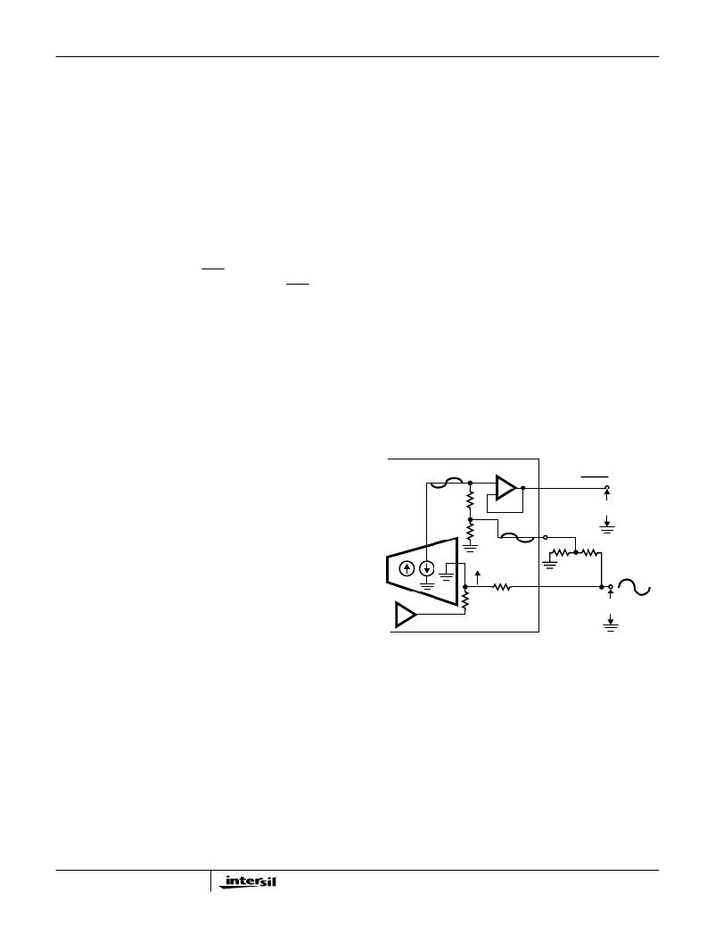
�Test� #8,� Transhybrid� Balance�
�This� test� will� illustrate� a� method� of� performing� transhybrid�
�balance� using� the� PTG� pin.� The� solution� is� to� use� the�
�P� rogrammable� T� ransmit� G� ain� pin� (PTG)� as� an� input� for� the�
�receive� signal� (V� RX� ).� When� the� PTG� pin� is� connected� to� a�
�divider� network� (R14� and� R15,� Figure� 5)� and� the� value� of� R14�
�and� R15� is� much� less� than� the� internal� 500k� ?� resistor� RB,� two�
�things� happen.� First,� the� transmit� gain� from� V� RX� to� V� TX� is�
�reduced� by� half.� This� is� the� result� of� shorting� out� the� bottom�
�500k� ?� resistor� with� the� much� smaller� external� resistor.� And�
�second,� the� input� signal� from� V� RX� is� also� divided� in� half� by�
�resistors� R14� and� R15.� Transhybrid� balance� occurs� when�
�these� two,� equal� but� opposite� in� phase,� signals� are� cancelled�
�at� the� input� to� the� output� buffer.�
�.�
�OUTPUT� BUFFER�
�simultaneously� across� a� complex� loop� resistance,� on� tip� and�
�-�
�V� TX�
�ring,� with� less� than� 1%� Total� Harmonic� Distortion.� The�
�complex� loop� impedance� is� equal� to� 200� ?� at� the� pulse�
�metering� frequency� of� 16kHz,� and� consist� of� a� series� 200� ?�
�resistor� and� a� parallel� combination� of� an� 820� ?� resistor� and� a�
�0.1� μ� F� capacitor.� Programming� of� the� offhook� overhead�
�I� X�
�RA�
�500K�
�RB�
�500K�
�+�
�A=1�
�PTG�
�R14�
�R15�
�-�
�V� TX�
�+�
�voltage� required� for� simultaneously� operation� of� both� signals�
�is� achieved� by� changing� the� value� of� RDC_RAC� to� 27.4k� ?� .�
�I� X�
�500K�
�V� RX�
�A� 27.4k� ?� RDC_RAC� resistor� (provided� with� kit),� two� signal�
�generators,� the� complex� load� listed� above� and� a� dynamic�
�signal� analyzer� are� required� to� complete� this� test.�
�5�
�500K�
�UniSLIC14�
�+�
�V� RX�
�-�
�Setup�
�1.� Connect� the� power� supplies� to� the� Evaluation� board.�
�2.� Set� V� BH� to� -48V,� V� BL� to� -24V� and� V� CC� to� +5V.�
�3.� Con?gure� the� SLIC� to� be� in� the� Forward� Active� state�
�(C3� =� 0,� C2� =� 1,� C1� =� 0).�
�4.� Verify� that� the� POL/REV� switch� S4� (lower� right� hand� side�
�of� the� board)� is� in� either� the� 10ms� or� 20ms� position.�
�5.� Change� R1� resistor� RDC_RAC� to� 27.4k� ?.�
�6.� Verify� that� pin� 2� of� the� PTG� jumper� (S8,� located� towards�
�the� middle� of� board� near� the� upper� right� hand� corner� of�
�the� SLIC)� is� shorted� to� pin� 1.� This� condition� grounds� the�
�PTG� pin.�
�FIGURE� 5.� TRANSHYBRID� BALANCE� USING� THE� PTG� PIN�
�Setup�
�1.� Connect� the� power� supplies� to� the� Evaluation� board.�
�2.� Set� V� BH� to� -48V,� V� BL� to� -24V� and� V� CC� to� +5V.�
�3.� Con?gure� the� SLIC� to� be� in� the� Forward� Active� State�
�(C3� =� 0,� C2� =� 1,� C1� =� 0).�
�4.� Verify� that� the� POL/REV� pin� S4� (lower� right� hand� side� of�
�the� board)� is� in� either� the� 10ms� or� 20ms� position.�
�5.� Terminate� tip� and� ring� with� a� 600� ?� load.�
�6.� Verify� that� pin� 2� of� the� PTG� jumper� (S8,� located� towards�
�the� middle� of� board� near� the� upper� right� hand� corner� of�
�the� SLIC)� is� short� to� pin� 3.� This� condition� connects�
�resistors� R14� and� R15� to� the� PTG� pin.�
�6�
�发布紧急采购,3分钟左右您将得到回复。
相关PDF资料
HC55185EVAL2
EVALUATION PLATFORM HC55185+T
HE1015
BOOT CIRCUIT BREAKER 1POLE CLEAR
HE1020
BOOT CIRCUIT BREAKER 2POLE CLEAR
HE1050
BOOT CIRCUIT BREAKER 3POLE CLEAR
HE1070
BOOT CIRCUIT BREAKER 3POLE CLEAR
HFW30R-1STE1
HFW30R-1STE1-FFC/FPC CONN
HFW30S-2STE1
HFW30S-2STE1-USING HFW-P5SL
HHG
FUSEHOLDER AUTO INLINE FOR ATC
相关代理商/技术参数
HC5515
制造商:INTERSIL 制造商全称:Intersil Corporation 功能描述:ITU CO/PABX SLIC with Low Power Standby
HC5515_06
制造商:INTERSIL 制造商全称:Intersil Corporation 功能描述:ITU CO/PABX SLIC with Low Power Standby
HC55150
制造商:INTERSIL 制造商全称:Intersil Corporation 功能描述:Low Power Universal SLIC Family
HC55150CB
制造商:Rochester Electronics LLC 功能描述:LOW PWR SLIC,POL REV/METERING,55DB BALANCE - Bulk
HC55150CBZ
功能描述:电信线路管理 IC LW PWR SLIC POLV/MTRING 55DB RoHS:否 制造商:STMicroelectronics 产品:PHY 接口类型:UART 电源电压-最大:18 V 电源电压-最小:8 V 电源电流:30 mA 最大工作温度:+ 85 C 最小工作温度:- 40 C 安装风格:SMD/SMT 封装 / 箱体:VFQFPN-48 封装:Tray
HC55150CM
制造商:Rochester Electronics LLC 功能描述:LOW PWR SLIC,POL REV/METERING,55DB BALANCE - Bulk
HC55150CMZ
功能描述:电信线路管理 IC LW PWR SLIC POLV/MTRING 55DB RoHS:否 制造商:STMicroelectronics 产品:PHY 接口类型:UART 电源电压-最大:18 V 电源电压-最小:8 V 电源电流:30 mA 最大工作温度:+ 85 C 最小工作温度:- 40 C 安装风格:SMD/SMT 封装 / 箱体:VFQFPN-48 封装:Tray
HC55151
制造商:INTERSIL 制造商全称:Intersil Corporation 功能描述:Low Power Universal SLIC Family